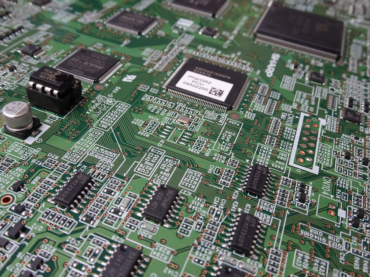
PCB layout
Schematic capture, HDI, multilayer, RF/microwave, flex and rigid-flex, with signal- and power-integrity analysis.
Idea to working prototype, fast - by engineers who design the board knowing exactly how it will be built. Mechanical fit, manufacturability and testing are considered from day one. New to the process? Start with our guide to choosing an electronics design & manufacturing partner.
Real strengths that shorten your timeline and de-risk the path to production.
Fast designing capability
Quick proof-of-concept and prototyping
Over 100 satisfied customers and products in the market
Post-design and post-manufacturing support
Mechanical integration handled at the PCB design stage itself
Engineers with a wide range of knowledge
Dedicated customer support
No reliance on a single supply chain - global and industrial holidays (e.g. Chinese New Year) do not affect us
Schematic capture, HDI, multilayer, RF/microwave, flex and rigid-flex, with signal- and power-integrity analysis.
System architecture, firmware, RTOS, FPGA/SoC and embedded software, validated end to end.
Low-power and precision analog, power converters, battery management, wireless and IoT integration.
DDRx, PCIe, MIPI, USB 2.0/3.0, HDMI, Ethernet and SATA.
Design-for-manufacture and assembly checks, IPC-compliant, to maximise yield and avoid surprises.
Quick-turn prototypes, full 3D product modelling and a clean path to high-volume production.
NDAs signed before you share a file, confidentiality agreements across the whole team, and secured, audited access to your data.
Request an NDA →Send us your concept and set up a call - we'll map the fastest, most reliable path from idea to production. NDAs welcome.